WashU physicists explain surprising findings from a cutting-edge quantum microscope, opening possibilities for advanced technologies.
Quantum materials are widely considered the building blocks of next-generation technologies, from quantum computing and advanced telecommunications to high-performance energy storage. But unlocking their potential requires more than powerful instruments. It demands theory to make sense of what those instruments reveal.
When researchers at the Weizmann Institute of Science in Rehovot, Israel, developed the Atomic Single Electron Transistor (Atomic SET), a groundbreaking quantum microscope that could probe materials using a single atom as a sensor, they knew they still only had part of the story.
As reported in Nature, the Israeli team turned to researchers at WashU to help develop a theory to explain the microscope’s readings, including many findings that didn’t align with the previous understanding of atomically thin quantum materials.

Using a new theoretical framework and massive computing power, Shaffique Adam, a professor of physics, and his team developed the model that made sense of the apparent anomalies. “We were able to explain their findings, which now give us a whole new understanding of the possibilities of quantum materials,” Adam said. The team also included WashU graduate student Liangtao Peng and Adam’s former PhD student Mohammed Al Ezzi.
The Atomic SET can measure electric properties with a spatial resolution of about one nanometer — roughly 100 times better than existing techniques. “The sensor can see things that have never been seen before,” Adam said.
The Israeli researchers tested the new device on a seemingly well-known quantum material, a two-dimensional layer of graphene stacked on a two-dimensional layer of hexagonal boron nitride. “They anticipated this would just be a boring test of the device because everyone thought this system was well understood,” Adam said. “But what they found was really unexpected.”
Hexagonal boron nitride layered with graphene had been used in many previous experiments, and the basic qualities were already well-established. The combination is intriguing for physicists because the atomic lattices in the two layers form a moiré pattern, a type of interference that creates new opportunities for atoms and electrons to interact with each other at the quantum level.
When the Israeli team probed the material with the Atomic SET, they quickly realized that the electric potential within the moiré pattern defied theoretical expectations. Specifically, the potential energy landscape — the energy required to move a charge against an electric field —exhibited unexpected symmetry and strong electric potential. “The prevailing theoretical picture anticipated small fluctuations in electric potential and a 120-degree rotation symmetry, which means that the patterns would stay the same if rotated 120 degrees,” Adam said. “Instead, the fluctuations were an order of magnitude higher than expected, and the symmetry was 60 degrees.”
Startled by these results, the team pored over the published literature looking for clues. They found a 2014 paper co-written by Adam, then at the National University of Singapore, that had used a continuum theory to predict strong electric potential in quantum materials. “Based on that paper, they asked us to look at their new results,” Adam said. “We developed a theoretical framework that accurately predicted the symmetry. We were also able to predict the size of the electric potential within a factor of two.”
Among other insights, Adam and his team realized that the sheets of graphene and hexagonal boron nitride weren’t acting like stiff, rigid sheets. “They’re more like membranes,” Adam said. “Membranes can relax, and the relaxation completely changes the symmetry properties of the material. We developed an analytical theory that allows us to predict these relaxed states with relatively small computational costs.”
Predicting the qualities of quantum materials is a crucial step toward applying the materials to technologies such as quantum computing, telecommunications, and advanced energy storage, Adam said. “We have thousands of new materials that can be stacked in multiple combinations, creating billions of possible new materials that didn't exist before,” he said. “But until now, we haven't had the predictive ability to be able to say which materials might be most effective for which uses. Understanding the interaction of relaxed moiré lattices is essential if we want to make rational choices to build reliable electronic structures.”
As a next step, Adam and his team hope to continue fine-tuning their theoretical models and applying them to data collected from other quantum materials. “We’ve shown that our methods work in a less exotic system,” Adam said. “We’re excited to work with the team at the Weizmann Institute and their state-of-the-art device to see what else we can discover.”
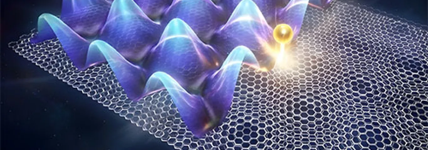
Header image: A tiny flaw in a material, just one misplaced atom, acts like a powerful new microscope. It lets scientists see the electric forces that guide how electrons move through quantum materials. (Image: Weizmann Institute of Science)